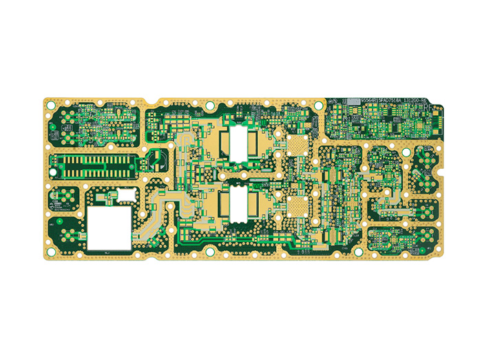
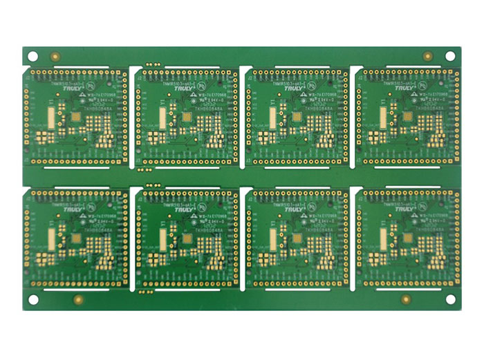
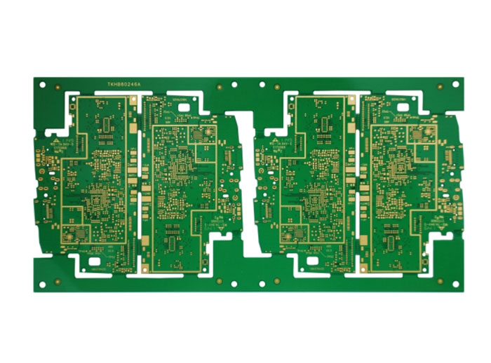
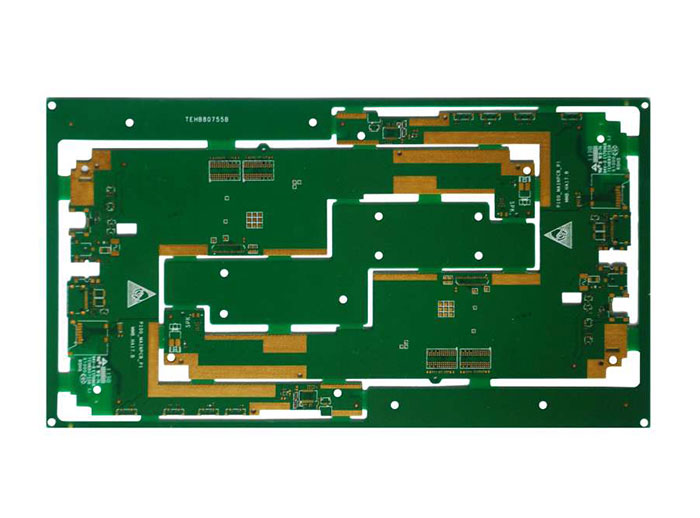
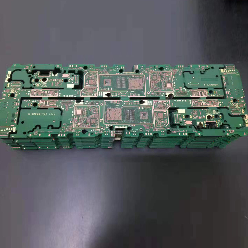
Product parameters
● Product name: 8-layer 1-level HDI board
● Type: HDI
● Material: FR4 high Tg
● Substrate copper foil thickness: 1oz outer layer; 1 / 3oz inner layer
● Minimum line width / space: 2mil / 2mil
● Minimum drilling hole diameter: 0.2mm
● Minimum laser drilling aperture: 0.075mm
● Blind hole depth ratio: 1: 1
● Maximum finished product size: 500mm X600mm
● Surface treatment: OSP + chemical immersion gold
● Solder mask color: green
● Special process: blind and buried hole
Detailed introduction
The definition of HDI (High Density Intrerconnection) circuit board refers to a microvia (Microvia) with a hole diameter of less than 6mil and a hole pad diameter of less than 0.25mm, a contact density of more than 130 points per square inch, and wiring Printed circuit boards with a density of more than 117 inches per square inch and a line width / pitch of less than 3mil / 3mil. HDI circuit boards are mainly used in different fields such as mobile phones, cameras, camcorders, notebook computers, network cards, IC carriers, military industries, and medical treatment.
Generally speaking, HDI circuit boards have the following advantages:
lower the cost
Increase wiring density
Facilitates the use of advanced packaging technology
Have better electrical performance and signal accuracy
Better reliability
May improve thermal properties
Can improve radio frequency interference, electromagnetic wave interference, electrostatic discharge
Increase design efficiency
HDI process capability
HDI type: first-order, second-order, third-order, arbitrary layer interconnection
Minimum line width / space: 2mil / 2mil
Minimum drilling hole diameter: 8mil (0.20mm)
Minimum laser drilling aperture: 3mil (0.075mm)
Blind hole depth ratio: 1: 1
Surface treatment: chemical immersion gold, immersion tin, immersion silver, full plate gold plating, OSP, lead-free tin spray, hard gold plating, gold fingers
Solder mask color: white, black, yellow, red, green, blue
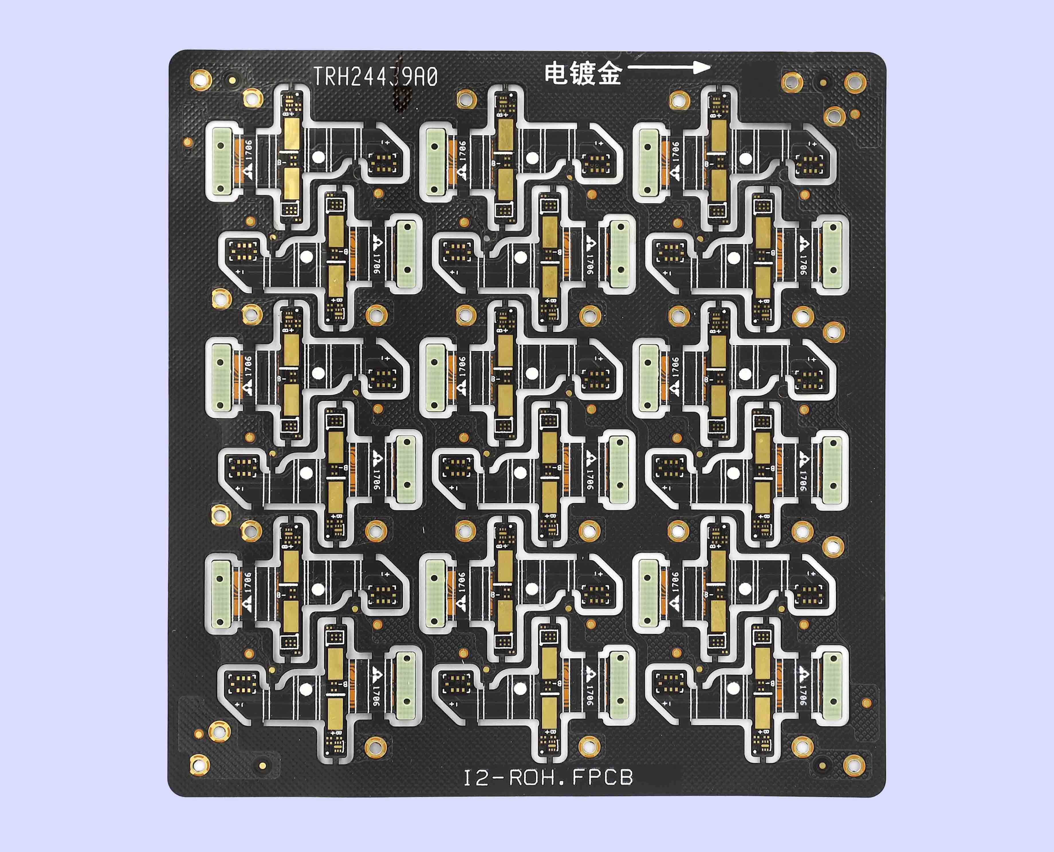
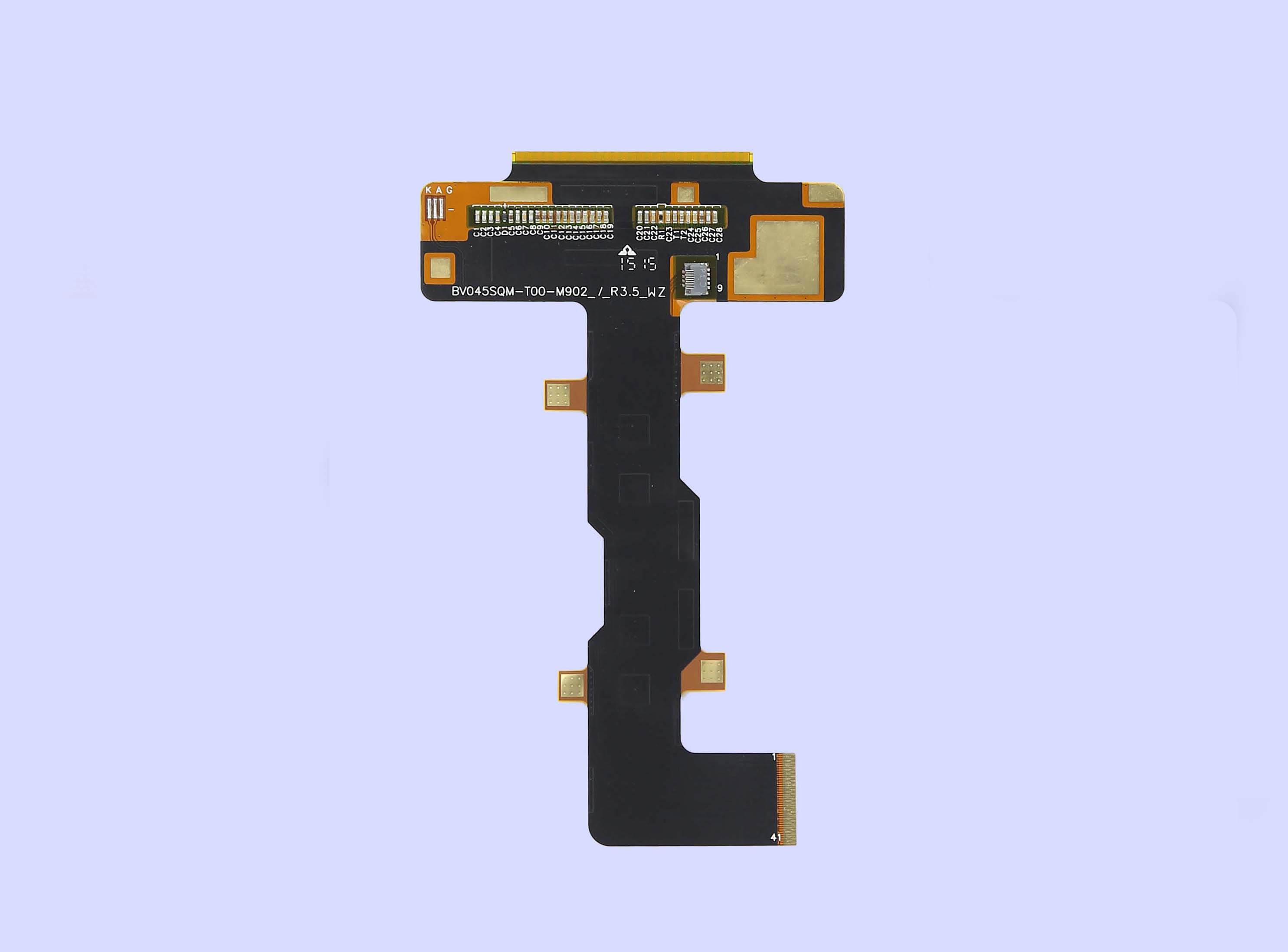
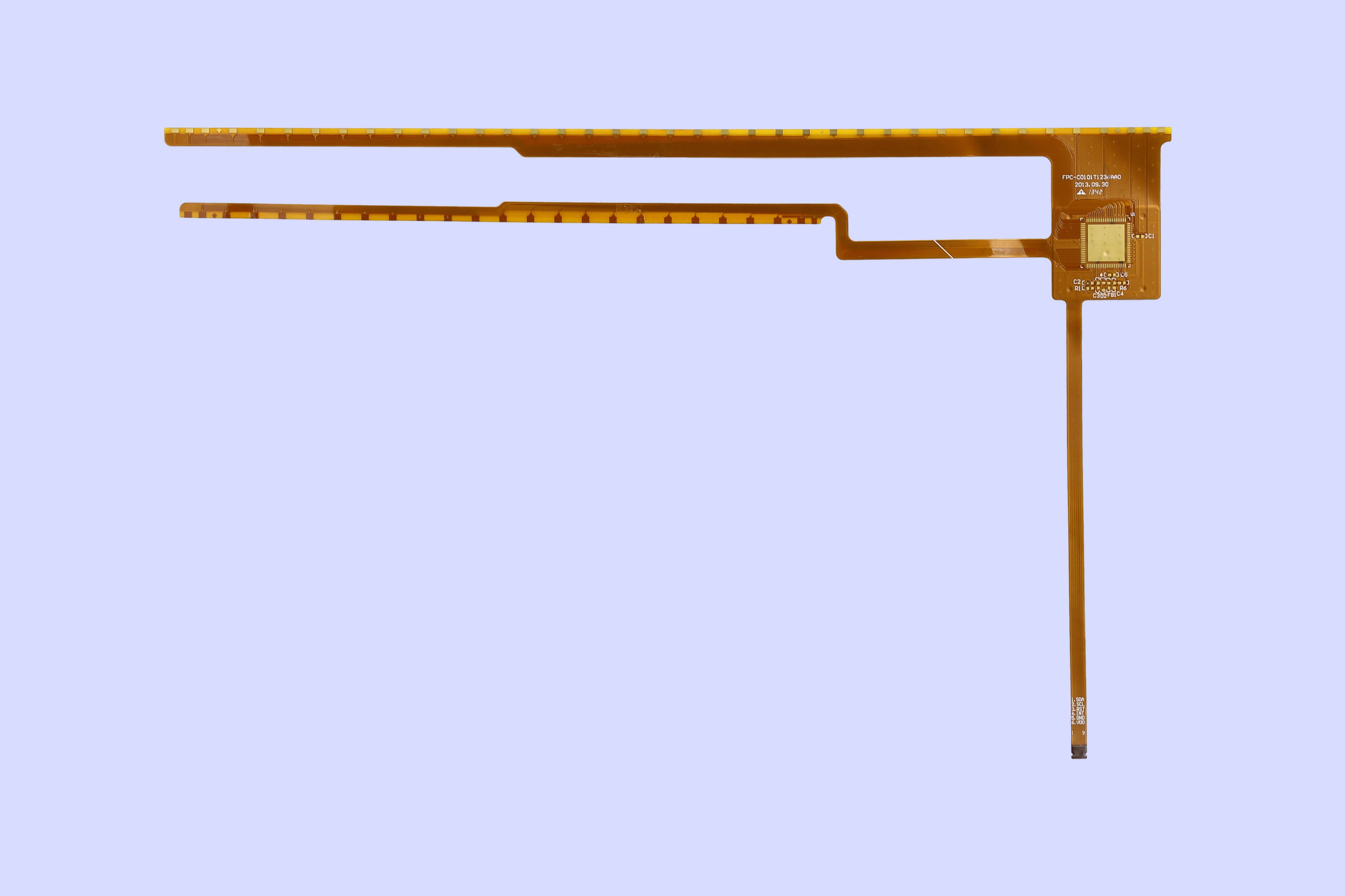
Product Details:


 Chinese